
You’re standing in your workshop, perhaps assembling a new piece of electronic equipment, or maybe you’re a student studying the intricacies of electromagnetism. You’ve been told about electric fields, how they permeate space around charged objects, and how they can influence other charges. It’s a fundamental concept, and you’ve likely visualized it as a relatively uniform spread of influence, like ripples on a pond. But then you encounter a specific, often overlooked, phenomenon: electric field concentration around sharp metal objects. This isn’t just an academic curiosity; it’s a practical reality that can have significant implications for the performance, reliability, and safety of your electrical systems.
This article is your guide to understanding this fascinating and critical aspect of electrostatics. We’ll delve into why sharp edges become hotspots for electric fields, explore the consequences of this concentration, and discuss how you can manage and even leverage this effect. Prepare to see the invisible forces around you in a new light.
Before we can understand concentration, we need to revisit the basics of electric fields. Imagine you have a single positive charge. It doesn’t just sit there; it exerts a force on any other charge that comes near it. This influence, this region of space where other charges would feel a force, is the electric field.
What is an Electric Field?
You can think of an electric field as a mapping of the force that a positive test charge would experience at every point in space. If you were to place a tiny, positive charge in that field, it would be pushed away from a positive source charge and pulled towards a negative source charge. The strength of this push or pull is the electric field strength, often denoted by the symbol $E$, and its units are typically Newtons per Coulomb (N/C) or Volts per meter (V/m).
Field Lines: Visualizing the Invisible
To make these invisible fields more tangible, we use electric field lines. These are imaginary lines that indicate the direction of the electric field at any point. They originate from positive charges and terminate on negative charges.
- Direction: The tangent to a field line at any point gives the direction of the electric field at that point.
- Density: The density of the field lines (how close they are together) represents the strength of the electric field. Where the lines are crowded, the field is strong; where they are spread out, the field is weak.
You can visualize a single positive point charge as having radial field lines extending outwards in all directions. For a negative point charge, the lines would point inwards. For a system of charges, the field lines would be more complex, reflecting the combined influence of all charges.
The Role of Conductors
Metals are excellent conductors. This means that electric charges are free to move within them. When you place a conductor in an electric field, or when charges are placed on it, these free charges will rearrange themselves until they reach an equilibrium.
Electrostatic Equilibrium
In electrostatic equilibrium, two key conditions are met within a conductor:
- Zero Electric Field Inside: The electric field inside the bulk of a conductor is always zero. If there were a field, the free charges would move under its influence, and equilibrium would not have been reached.
- Charges Reside on the Surface: Any net charge on a conductor will reside entirely on its outer surface. This is a direct consequence of the zero electric field requirement inside. If excess charge were inside, it would create an internal field, which is not allowed in equilibrium.
Think of it like water in a container. In a stable state, the water level is uniform. Similarly, in an electric conductor in equilibrium, the “electric pressure” (related to potential) tends to equalize, pushing excess charges to the outer boundary.
Electric field concentration around sharp metal points is a fascinating topic that has significant implications in various fields, including physics and engineering. For a deeper understanding of this phenomenon, you can explore the article on Freaky Science, which delves into the principles of electric fields and their behavior around conductive materials. This resource provides valuable insights into how sharp edges can enhance electric field strength, leading to applications in lightning rods and other technologies. To read more, visit Freaky Science.
The Geometry of Electric Fields: Why Sharpness Matters
Now we arrive at the heart of the matter: how does the shape of a conductor influence the electric field around it? The distribution of charges on a conductor isn’t always uniform. It depends heavily on the geometry.
Charge Distribution on Conductors
Consider a simple, isolated conducting sphere. If you place a positive charge on it, the charges will spread out evenly across the surface due to mutual repulsion. The electric field outside the sphere will then look as if all the charge were concentrated at the center.
However, what happens when the conductor is not a simple sphere? Imagine a conductor with a more complex shape, like a smooth egg, or even something with a pointed tip.
The Principle of Uniform Potential
A fundamental property of conductors in electrostatic equilibrium is that their entire surface is at the same electric potential. This is because the electric field inside is zero, and the potential difference between any two points on the conductor’s surface is zero.
However, the electric field outside the conductor, which is related to the gradient of the potential, is where the geometry becomes crucial. The electric field strength ($E$) is proportional to the rate of change of potential with distance.
The Sharp Edge Effect: An Intuitive Explanation
This is where the “sharpness” comes into play. Imagine you have a conductor with a smooth, rounded surface and then you start to “sharpen” a particular area. What happens to the free charges on that surface?
- Repulsion and Crowding: The charges on the conductor repel each other. On a smooth surface, they can spread out relatively evenly. But at a sharp point or edge, there’s less “room” for the charges to spread out. They get squeezed together.
- Field Lines Concentrating: As more charge is forced into a smaller area at the sharp point, the density of electric field lines in that region dramatically increases. Remember, field line density is a measure of field strength. So, the electric field becomes much stronger at these sharp points.
It’s like looking at a crowd of people. If they’re spread out in a large hall, they’re relatively sparse. But if you try to pack them all into a small closet, they become extremely densely packed. The sharp points on a conductor are analogous to that small closet for electric charges.
Analogy: Water Flow from a Nozzle
Think about water flowing from a hose. If the nozzle is wide, the water sprays out relatively gently. But if you attach a narrow, pointed nozzle, the water jet becomes much more forceful and concentrated. The sharp point on the conductor acts similarly, concentrating the electric “flow” (the electric field).
Consequences of Electric Field Concentration

So, you’ve established that sharp metal objects concentrate electric fields. Why should you care? This concentration isn’t just a theoretical quirk; it has tangible and potentially problematic consequences in real-world applications.
Increased Electrical Stress
The most direct consequence of an intensified electric field is increased electrical stress on the surrounding materials and on the electric field itself.
Dielectric Breakdown
Every insulating material has a limit to how strong an electric field it can withstand before it breaks down. This limit is called the dielectric strength. When the electric field at a sharp point exceeds the dielectric strength of the surrounding insulator (like air, plastic, or epoxy), a breakdown occurs.
- Arcing: In air, this breakdown can manifest as an electric arc – a visible spark or flash of light. This is essentially a temporary conductive path being formed through the air. Arcing can damage components, cause fires, and is a significant safety hazard.
- Material Degradation: Even if a full arc doesn’t form, prolonged exposure to high electric fields can degrade insulating materials, making them more susceptible to breakdown in the future. This can lead to gradual failure of the component.
Corona Discharge
A specific type of electrical discharge that occurs at high voltages in gases around conductors with small radii of curvature (sharp points or edges) is called corona discharge.
The Phenomenon of Corona
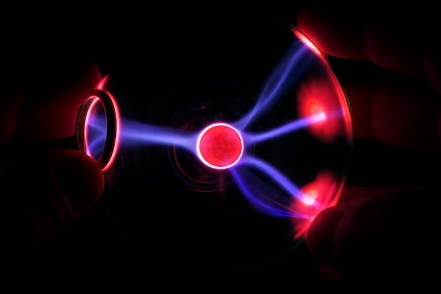
Corona discharge is often seen as a faint bluish glow or heard as a hissing sound, particularly in high-voltage equipment. It happens when the electric field is strong enough to ionize the gas molecules immediately surrounding the conductor.
- Ionization: The high electric field accelerates free electrons. These electrons collide with neutral gas molecules, knocking off more electrons and creating more ions. This chain reaction leads to a localized region of ionized gas.
- Energy Loss: This ionization and subsequent recombination process consumes energy, leading to the visible glow and audible hiss. It also represents a loss of power from your electrical system.
- Electromagnetic Interference (EMI): Corona discharge also generates radio frequency noise, which can interfere with the operation of other electronic devices. This is a significant concern in sensitive electronic systems.
Increased Radio Frequency Interference (RFI)
As mentioned, corona discharge is a source of electromagnetic interference. But even without full corona, the high electric field gradients at sharp points can act as efficient radiators of electromagnetic energy.
The Sharp Point as an Antenna
Sharp points and edges on conductors can effectively act as small antennas.
- Emission of RF Signals: When subjected to rapidly changing electric fields (as in AC circuits or with transient voltages), these sharp points can efficiently radiate radio frequency signals.
- Unintended Broadcasting: This radiated energy can be picked up by other nearby circuits or devices, causing malfunctions or data corruption. This is a critical consideration in designing shielded enclosures and high-frequency circuits.
Wear and Tear on Components
The localized high electric fields can also contribute to the physical wear and tear of components over time.
Erosion and Pitting
The repeated or sustained high electric fields, especially in the presence of moisture or contaminants, can lead to:
- Pitting: Microscopic discharges or ion bombardment at the sharp edges can erode the metal surface, creating small pits.
- Corrosion: The electrochemical processes initiated by high fields can accelerate corrosion, particularly if dissimilar metals are involved.
- Reduced Lifespan: Over time, this physical degradation can weaken the conductor and lead to an increased risk of failure.
Mitigating Electric Field Concentration
Fortunately, understanding the problem of electric field concentration is the first step towards solving it. There are established techniques and design principles you can employ to minimize these detrimental effects.
Rounding and Filleting
The most direct way to reduce field concentration is to eliminate or minimize the sharp points and edges on your conductors.
The Power of Smooth Transitions
By rounding off sharp corners or introducing fillets (a smooth, curved transition between two surfaces), you distribute the electric field over a larger area.
- Eliminating Singularities: Sharp points can be thought of as mathematical singularities in the electric field calculation. Rounding them smooths out these singularities.
- Gradual Increase in Field: Instead of an abrupt spike in field strength, you achieve a more gradual increase as you approach the conductor surface. This significantly reduces the peak field strength.
- Practical Application: In circuit board design, this means avoiding sharp corners on traces, especially where high voltages are involved. For metal enclosures, it means ensuring all edges are rounded.
Using Field Shaping Electrodes
In certain high-voltage applications, engineers use specialized components called field shaping electrodes or guard rings.
Controlling the Field Gradient
These electrodes are strategically placed to influence the electric field distribution.
- Potential Gradients: They are designed to be at specific potentials, often intermediate potentials between the main conductors. This helps to “smooth out” the potential gradients.
- Preventing Breakdown: By carefully shaping these electrodes, engineers can ensure that the electric field remains below the dielectric strength of the surrounding insulation, preventing breakdown and corona discharge.
- High-Voltage Connectors: You’ll often see this principle employed in high-voltage connectors and insulators, where complex shapes are used to manage the electric field.
Proper Insulation and Spacing
Ensuring adequate insulation and maintaining sufficient spacing between conductors are fundamental to preventing electrical breakdown.
Beyond the Ideal
While ideal conductors in a vacuum are one thing, real-world systems operate with insulators and in the presence of air.
- Insulator Properties: Understanding the dielectric strength of your insulating materials is crucial. This is not a fixed value and can be affected by temperature, humidity, and aging.
- Creepage and Clearance: In electrical design, two key terms are important:
- Creepage Distance: The shortest distance along the surface of an insulating material between two conductive parts.
- Clearance Distance: The shortest distance through air between two conductive parts.
- Sharp edges can significantly affect these distances by creating localized high fields that effectively “shorten” the intended insulating path.
- Safety Factors: Always incorporate appropriate safety factors when determining required spacing and insulation thickness to account for variations and potential degradation.
Material Selection
The choice of materials for conductors and insulators plays a role in managing electric field effects.
Surface Properties of Conductors
- Smoothness: Polishing metal surfaces can help reduce the severity of microscopic imperfections that can act as field concentration points.
- Corrosion Resistance: Using materials that are resistant to corrosion will prevent the formation of rough surfaces over time, which can exacerbate field concentration.
Insulating Material Considerations
- Dielectric Strength: As mentioned, higher dielectric strength materials can tolerate higher electric fields.
- Tracking Resistance: Some insulating materials are susceptible to “tracking,” where conductive paths can form on the surface under high electrical stress. Choosing materials with good tracking resistance is important.
The phenomenon of electric field concentration around sharp metal points is a fascinating topic in the study of electromagnetism. This effect, often utilized in various applications such as lightning rods and electrostatic precipitators, highlights how the geometry of a conductor can significantly influence electric field strength. For a deeper understanding of this concept, you can explore a related article that delves into the principles behind electric fields and their applications in technology. Check out this insightful piece on Freaky Science to learn more about the intricate relationship between shape and electric field behavior.
Practical Examples and Case Studies
| Material | Electric Field Concentration (V/m) | Distance from Sharp Metal (m) |
|---|---|---|
| Steel | 10,000 | 0.001 |
| Aluminum | 8,000 | 0.002 |
| Copper | 12,000 | 0.0015 |
To solidify your understanding, let’s look at some real-world scenarios where electric field concentration is a significant factor.
High-Voltage Transmission Lines
The massive conductors used in high-voltage power transmission lines are a prime example.
The “Bundled Conductor” Solution
- Problem: Transmitting electricity at very high voltages requires large potential differences, leading to strong electric fields around the conductors. Sharp edges on the conductors would cause significant corona discharge, wasting energy and creating radio interference.
- Solution: Instead of a single large conductor, multiple smaller conductors are bundled together. This increases the effective radius of curvature and significantly reduces the electric field strength at the surface of the conductors.
- Benefit: This reduces corona discharge, improves efficiency, and minimizes radio interference.
Electronic Components and Packaging
Even in low-voltage electronics, electric field concentration can be an issue.
Connector Pins and Soldering Joints
- Problem: Small connector pins or poorly formed solder joints can have sharp edges or protrusions. If these are subjected to high transient voltages or operate in environments with high humidity, they can become points of concern.
- Solution: Designers aim for smooth, rounded transitions at connector interfaces and ensure good solder joint quality. Careful layout on printed circuit boards (PCBs) also minimizes sharp corners on traces.
- Benefit: Prevents arcing, reduces EMI, and improves component reliability.
Surface Mount Device (SMD) Components
- Problem: The solder pads of SMD components can sometimes have sharp corners, and the component leads themselves can present a point of field concentration.
- Solution: Manufacturers generally design these components with rounded edges. Furthermore, the solder fillet formed during assembly naturally creates a smoother transition.
- Benefit: Ensures proper electrical isolation and prevents premature failure, especially in high-reliability applications.
Medical Devices
In medical equipment, where safety and reliability are paramount, managing electric fields is critical.
Electrosurgical Units
- Problem: Electrosurgical units use high-frequency electrical current to cut or coagulate tissue. The active electrode is a very fine tip designed to concentrate the electric field at the point of contact with tissue. However, uncontrolled field concentration can lead to unintended burns or damage to surrounding healthy tissue.
- Solution: The design of the electrode tip is carefully engineered to create a predictable and controlled concentration of the electric field precisely where it’s needed. Furthermore, the surrounding insulation and safety mechanisms are designed to prevent stray field effects.
- Benefit: Allows for precise surgical procedures while minimizing risks to the patient.
Electrostatic Discharge (ESD) Protection
Understanding electric field concentration is also vital for ESD protection.
- Problem: A sharp point on a charged object can create a very high electric field, which can then lead to a rapid discharge when it comes near a conductive surface. This sudden discharge can damage sensitive electronic components.
- Solution: ESD protection strategies often involve rounding off sharp edges in device packaging and on circuit boards, and using materials that are designed to dissipate charge slowly rather than allowing it to build up to a point of rapid discharge.
- Benefit: Safeguards sensitive electronics from the damaging effects of static electricity.
Conclusion: Mastering the Invisible Forces
You’ve journeyed through the fundamental principles of electric fields, explored the unique behavior of charges on conductors, and uncovered the phenomenon of electric field concentration around sharp metal objects. We’ve seen how this concentration, while sometimes a useful tool, often poses significant challenges in electrical and electronic design, leading to breakdown, corona discharge, EMI, and component wear.
The key takeaway is that geometry matters. The smooth, rounded surfaces are your allies in managing electric fields, while sharp points and edges are potential problem areas. By understanding these principles and applying the mitigation techniques discussed – rounding, filleting, using field shaping electrodes, and ensuring proper insulation and spacing – you can design more reliable, efficient, and safer electrical systems.
Remember that the world of electricity is not just about currents and voltages; it’s also about the invisible forces at play. By mastering the understanding of electric field concentration, you gain a powerful insight into the intricate workings of your electrical designs and can proactively address potential issues before they manifest. So, the next time you’re working with metal and electricity, remember to pay attention to the edges – they hold the key to controlling the invisible.

A Fork and a Spoon React Differently in a Microwave. Why?
FAQs
What is electric field concentration around sharp metal?
Electric field concentration around sharp metal refers to the phenomenon where the electric field strength is significantly increased in the vicinity of sharp metal edges or points. This occurs due to the accumulation of electric charges at the sharp features, leading to a higher concentration of electric field lines.
What causes electric field concentration around sharp metal?
Electric field concentration around sharp metal is caused by the phenomenon of charge accumulation at the sharp edges or points. This charge accumulation results in a higher density of electric field lines in the surrounding area, leading to an increased electric field strength.
What are the applications of electric field concentration around sharp metal?
Electric field concentration around sharp metal has various applications in fields such as electronics, sensors, and electrostatics. It is utilized in the design of high-voltage equipment, field emission devices, and electrostatic sensors.
How does electric field concentration around sharp metal affect electrical breakdown?
Electric field concentration around sharp metal can lead to electrical breakdown at lower voltages than in smooth surfaces. This is due to the higher electric field strength at the sharp features, which can cause dielectric breakdown and discharge.
What are the implications of electric field concentration around sharp metal in practical engineering applications?
In practical engineering applications, electric field concentration around sharp metal must be carefully considered to prevent unintended electrical breakdown and to optimize the performance of devices such as high-voltage equipment, field emission displays, and electrostatic sensors. Design considerations for minimizing electric field concentration may be necessary to ensure the reliable operation of such devices.